
Semiconductor Process and Packaging Cutting Guides
Application guidance for semiconductor process tapes, assembly films and advanced packaging materials, with practical review points for blade selection, clean edges, particle control and dimensional accuracy.
Coverage at a glance
60 application guides in this industry hub.
Materials covered
- ABF build-up film
- wafer mounting tape
- temporary wafer-bonding film
- package-substrate solder-mask dry film
- DBG process dicing tape
- fan-out wafer-level packaging film
Cutting processes
- roll slitting
- razor slitting
- kiss cutting
- transverse cross cutting
- shear slitting
- rotary die cutting
Common cut-quality risks
- Slit width drifts across the web
- The cut edge shows adhesive transfer, backing stretch, liner cut-through, edge lift or particulate contamination
- The cut edge shows layer lift, edge contamination, wrinkling, adhesive stringing or dimensional drift
- Film stretches, wrinkles or shifts registration
- Finished dimensions drift during a production run
- The workpiece shifts, curls or loses functional surface quality
Browse focused application knowledge
Cutting guides by industry, process, equipment and defect
Use these curated topic pages to compare related materials and cutting conditions without relying on broad site search.
Industries
Cutting processes
Equipment types
Cutting defects
Products and services
Related Products and Custom Services
These options are most frequently connected to the application guides in this topic.
Custom Knives
35 guides in this topic reference this option.
Circular Slitter Blades & Rotary Knives
19 guides in this topic reference this option.
Industrial Film Slitting Blade
6 guides in this topic reference this option.
Technical Articles
Industrial cutting problem knowledge base
1495 Blade Application Guides
Search by material, industry, cutting process or a problem described in your own words. You do not need to know the exact blade name.

Semiconductor Process & Packaging
ABF Build-Up Film Roll Slitting Blades
Application guide for ABF build-up film roll slitting, focused on slit width drifts across the web, film stretches, wrinkles or shifts registration, dimensional control and the production details needed for an RFQ.
Read the application guide →
Semiconductor Process & Packaging
ABF Build-Up Film Transverse Cross Cutting Blades
Application guide for ABF build-up film transverse cross cutting, focused on length or squareness changes at production speed, film stretches, wrinkles or shifts registration, dimensional control and the production details needed for an RFQ.
Read the application guide →
Semiconductor Process & Packaging
ABF Build-Up Film Width Edge Trimming Blades
Application guide for ABF build-up film width edge trimming, focused on trim ribbon breaks or returns to the product web, film stretches, wrinkles or shifts registration, dimensional control and the production details needed for an RFQ.
Read the application guide →
Semiconductor Process & Packaging
ABF Build-Up Film Rotary Die Cutting Blades
Application guide for ABF build-up film rotary die cutting, focused on waste matrix breaks or lifts finished parts, film stretches, wrinkles or shifts registration, dimensional control and the production details needed for an RFQ.
Read the application guide →
Semiconductor Process & Packaging
Package-Substrate Solder-Mask Dry Film Roll Slitting Blades
Application guide for package-substrate solder-mask dry film roll slitting, focused on slit width drifts across the web, film stretches, wrinkles or shifts registration, dimensional control and the production details needed for an RFQ.
Read the application guide →
Semiconductor Process & Packaging
Package-Substrate Solder-Mask Dry Film Transverse Cross Cutting Blades
Application guide for package-substrate solder-mask dry film transverse cross cutting, focused on length or squareness changes at production speed, film stretches, wrinkles or shifts registration, dimensional control and the production details needed for an RFQ.
Read the application guide →
Semiconductor Process & Packaging
Package-Substrate Solder-Mask Dry Film Width Edge Trimming Blades
Application guide for package-substrate solder-mask dry film width edge trimming, focused on trim ribbon breaks or returns to the product web, film stretches, wrinkles or shifts registration, dimensional control and the production details needed for an RFQ.
Read the application guide →
Semiconductor Process & Packaging
Package-Substrate Solder-Mask Dry Film Rotary Die Cutting Blades
Application guide for package-substrate solder-mask dry film rotary die cutting, focused on waste matrix breaks or lifts finished parts, film stretches, wrinkles or shifts registration, dimensional control and the production details needed for an RFQ.
Read the application guide →
Semiconductor Process & Packaging
Wafer Backgrinding Tape Roll Slitting Blades
Application guide for wafer backgrinding tape roll slitting, focused on slit width drifts across the web, film stretches, wrinkles or shifts registration, dimensional control and the production details needed for an RFQ.
Read the application guide →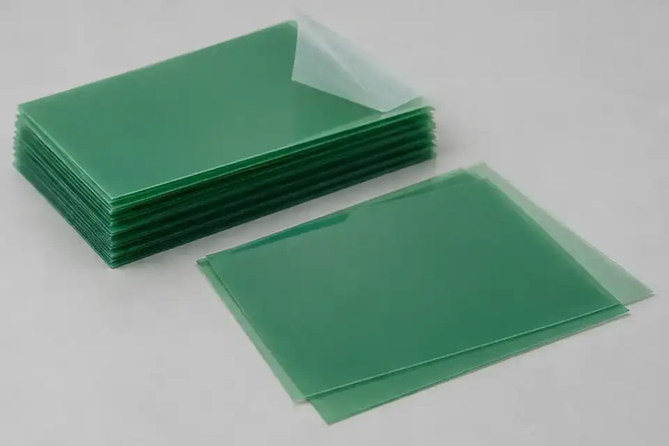
Semiconductor Process & Packaging
Wafer Backgrinding Tape Transverse Cross Cutting Blades
Application guide for wafer backgrinding tape transverse cross cutting, focused on length or squareness changes at production speed, film stretches, wrinkles or shifts registration, dimensional control and the production details needed for an RFQ.
Read the application guide →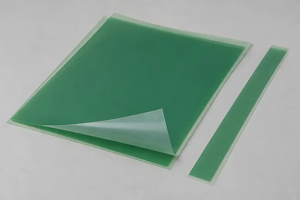
Semiconductor Process & Packaging
Wafer Backgrinding Tape Width Edge Trimming Blades
Application guide for wafer backgrinding tape width edge trimming, focused on trim ribbon breaks or returns to the product web, film stretches, wrinkles or shifts registration, dimensional control and the production details needed for an RFQ.
Read the application guide →
Semiconductor Process & Packaging
Wafer Backgrinding Tape Rotary Die Cutting Blades
Application guide for wafer backgrinding tape rotary die cutting, focused on waste matrix breaks or lifts finished parts, film stretches, wrinkles or shifts registration, dimensional control and the production details needed for an RFQ.
Read the application guide →
Semiconductor Process & Packaging
Die Attach Film Roll Slitting Blades
Application guide for die attach film roll slitting, focused on slit width drifts across the web, film stretches, wrinkles or shifts registration, dimensional control and the production details needed for an RFQ.
Read the application guide →
Semiconductor Process & Packaging
Die Attach Film Transverse Cross Cutting Blades
Application guide for die attach film transverse cross cutting, focused on length or squareness changes at production speed, film stretches, wrinkles or shifts registration, dimensional control and the production details needed for an RFQ.
Read the application guide →
Semiconductor Process & Packaging
Die Attach Film Width Edge Trimming Blades
Application guide for die attach film width edge trimming, focused on trim ribbon breaks or returns to the product web, film stretches, wrinkles or shifts registration, dimensional control and the production details needed for an RFQ.
Read the application guide →
Semiconductor Process & Packaging
Die Attach Film Rotary Die Cutting Blades
Application guide for die attach film rotary die cutting, focused on waste matrix breaks or lifts finished parts, film stretches, wrinkles or shifts registration, dimensional control and the production details needed for an RFQ.
Read the application guide →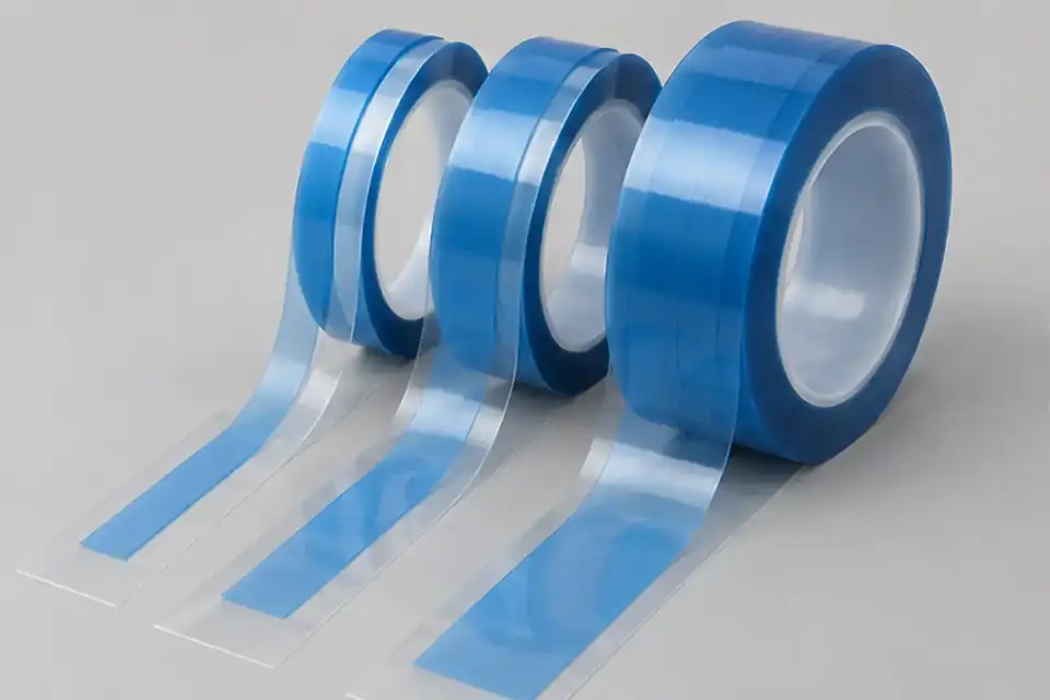
Semiconductor Process & Packaging
Thermal Interface Graphite Sheet Roll Slitting Blades
Application guide for thermal interface graphite sheet roll slitting, focused on slit width drifts across the web, film stretches, wrinkles or shifts registration, dimensional control and the production details needed for an RFQ.
Read the application guide →
Semiconductor Process & Packaging
Thermal Interface Graphite Sheet Transverse Cross Cutting Blades
Application guide for thermal interface graphite sheet transverse cross cutting, focused on length or squareness changes at production speed, film stretches, wrinkles or shifts registration, dimensional control and the production details needed for an RFQ.
Read the application guide →
Semiconductor Process & Packaging
Thermal Interface Graphite Sheet Width Edge Trimming Blades
Application guide for thermal interface graphite sheet width edge trimming, focused on trim ribbon breaks or returns to the product web, film stretches, wrinkles or shifts registration, dimensional control and the production details needed for an RFQ.
Read the application guide →
Semiconductor Process & Packaging
Thermal Interface Graphite Sheet Rotary Die Cutting Blades
Application guide for thermal interface graphite sheet rotary die cutting, focused on waste matrix breaks or lifts finished parts, film stretches, wrinkles or shifts registration, dimensional control and the production details needed for an RFQ.
Read the application guide →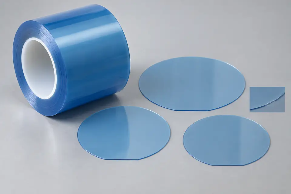
Semiconductor Process & Packaging
Wafer Mounting Tape Razor Slitting Blades
Application guide for wafer mounting tape razor slitting, focused on the cut edge shows adhesive transfer, backing stretch, liner cut-through, edge lift or particulate contamination, finished dimensions drift during a production run, dimensional control and the production details needed for an RFQ.
Read the application guide →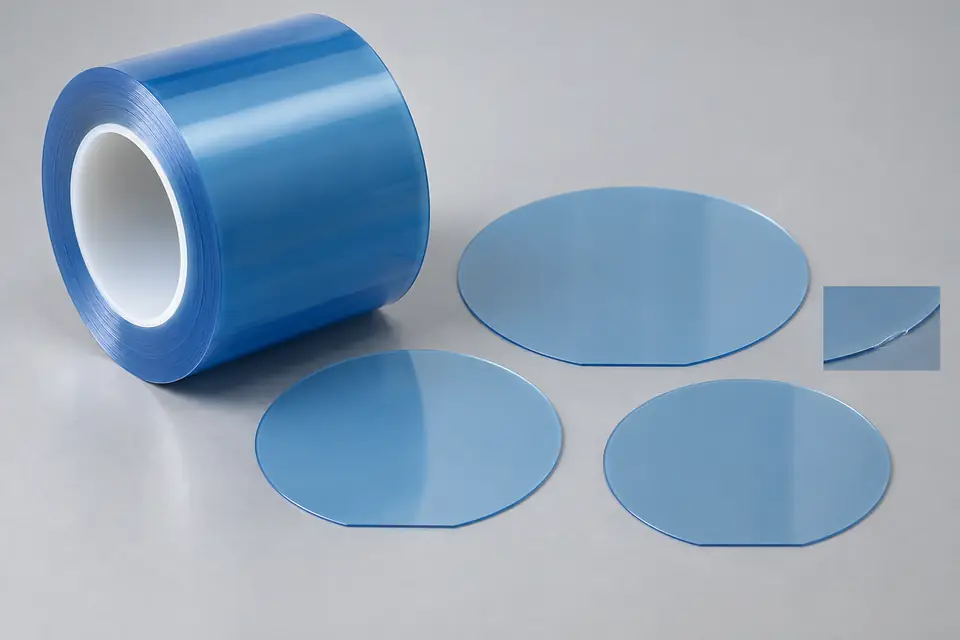
Semiconductor Process & Packaging
Wafer Mounting Tape Shear Slitting Blades
Application guide for wafer mounting tape shear slitting, focused on the cut edge shows adhesive transfer, backing stretch, liner cut-through, edge lift or particulate contamination, finished dimensions drift during a production run, dimensional control and the production details needed for an RFQ.
Read the application guide →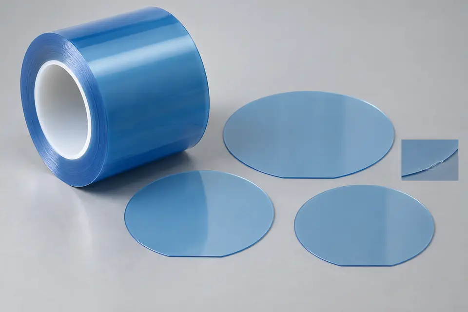
Semiconductor Process & Packaging
Wafer Mounting Tape Kiss-Cutting Blades
Application guide for wafer mounting tape kiss cutting, focused on the cut edge shows adhesive transfer, backing stretch, liner cut-through, edge lift or particulate contamination, finished dimensions drift during a production run, dimensional control and the production details needed for an RFQ.
Read the application guide →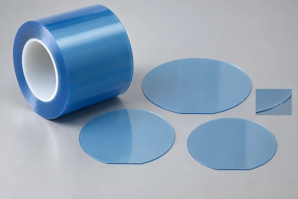
Semiconductor Process & Packaging
Wafer Mounting Tape Precision Cross-Cutting Blades
Application guide for wafer mounting tape precision cross cutting, focused on the cut edge shows adhesive transfer, backing stretch, liner cut-through, edge lift or particulate contamination, finished dimensions drift during a production run, dimensional control and the production details needed for an RFQ.
Read the application guide →Industrial Blade Application Guides: From Material to Cutting Edge
Reliable cutting comes from a system, not a single hardness number. Industrial blade technology connects the processed material, cutting method, machine condition, blade material, heat treatment, geometry, grinding accuracy and maintenance practice.
This page gives engineers and buyers a practical framework for discussing blade performance with Meirente before a quotation, trial or repeat-order improvement.
Start With the Cutting Application
A thin film, abrasive glass fiber, soft food product, polymer strand and electronic ceramic sheet place very different demands on a blade. The first questions should cover material behavior, thickness, speed, cutting gap, temperature, contamination, target finish and the cost of downtime.
Material Selection Is a Balance
Tool steel, stainless steel, high-speed steel, powder-metallurgy grades, tungsten carbide and coated solutions offer different combinations of hardness, toughness, wear resistance, corrosion resistance and cost. Selection should reflect the dominant failure risk instead of using the same grade for every application.
Edge Geometry Controls How the Blade Enters the Material
Bevel angle, single- or double-bevel direction, edge thickness, tooth pitch, tooth height, rake and clearance influence cutting force, dust, burrs, heat and edge strength. A sharper edge can reduce force, but an edge that is too thin may chip or deform under impact.
Heat Treatment, Grinding and Surface Engineering
Heat treatment develops the material properties required by the design. Precision grinding then controls flatness, parallelism, runout, concentricity and final edge geometry. Surface finishing or coating may help with wear, friction, corrosion or material adhesion when the application and base material justify it.
Measurement and Failure Feedback
Inspection confirms whether the blade matches the agreed specification; production feedback confirms whether the specification matches the real process. Photos and records of wear, chipping, deformation, burrs, dust, motor load, heat and cutting hours help separate material problems from alignment, gap, vibration or contamination issues.
Is higher hardness always better?
No. Higher hardness can improve wear resistance but may reduce toughness. The correct balance depends on impact, material abrasiveness and machine stability.
Why does the same blade wear differently on two machines?
Alignment, holder condition, cutting gap, speed, cooling, vibration, contamination and processed material can all change blade life.
When should a coating be considered?
Consider it when wear, friction, corrosion or adhesion is a defined problem and the coating is compatible with the base material, edge and operating temperature.
What information helps diagnose chipping?
Provide the chipped location, installation direction, holder condition, cutting gap, speed, processed material, contamination risk and close-up photos.
Can edge geometry be changed without changing the machine?
Sometimes, but the blade-holder interface, clearance and cutting method must be reviewed before any geometry change is approved.