
Blade Application Guides / Application Guide / Semiconductor fabrication
Semiconductor Molding Protection Tape Kiss-Cutting Blades
Semiconductor Molding Protection Tape is a cleanroom adhesive tape whose backing, adhesive layer and release behavior must remain stable during wafer handling. For kiss cutting, review Semiconductor Molding Protection Tape composition, grade, thickness and allowable lot variation, Layer, coating, porosity, temper, adhesive or surface-function details relevant to kiss cutting, support, operating speed and the actual equipment interface together. Compare accepted and rejected samples for the cut edge shows adhesive transfer, backing stretch, liner cut-through, edge lift or particulate contamination and finished dimensions drift during a production run before confirming a knife configuration.
Reviewed by the MEIRENTE technical team · Updated September 13, 2026
Where This Cutting Application Appears
Semiconductor fabrication production
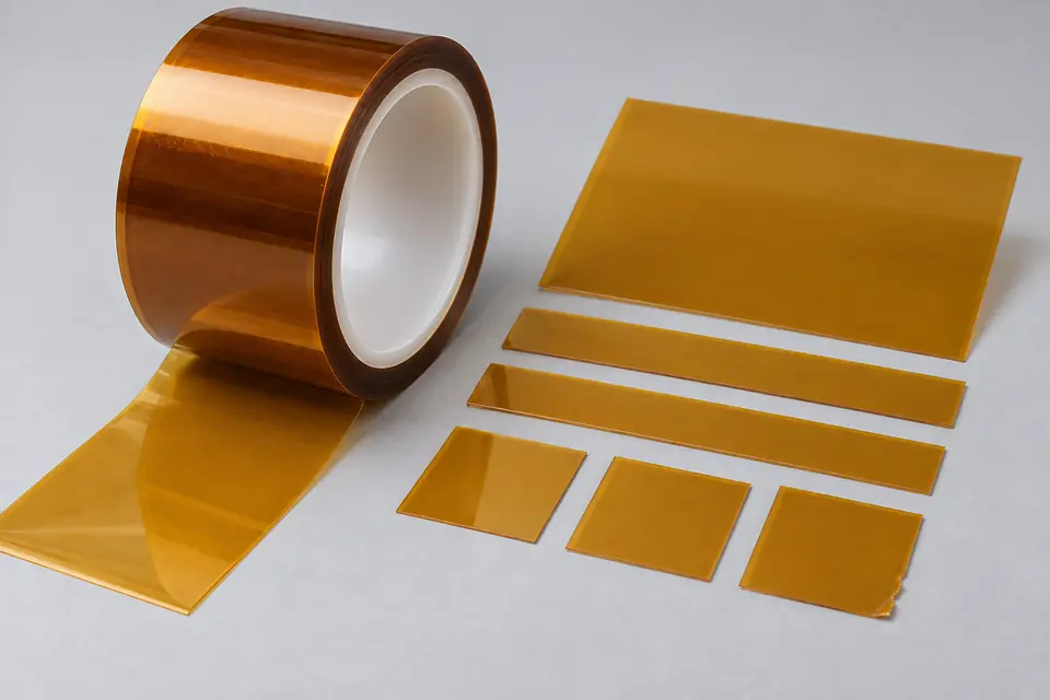
Semiconductor Molding Protection Tape is processed by kiss cutting to support wafer mounting, dicing, molding protection and temporary process support. The finished geometry must remain compatible with downstream handling and assembly.
Cut-quality control
Production teams compare accepted and rejected samples for cut width, edge cleanliness, adhesive residue, liner condition, particle level and dimensional stability, then relate the result to penetration depth, liner thickness, support pressure, registration and release behavior.
Stable material and waste handling
clean contact surfaces, controlled web tension and protected collection of converted tape help the product and waste leave the cut zone consistently without creating a second defect after separation.
Common Ways to Describe This Cutting Problem
- semiconductor molding protection tape kiss-cutting blades
- industrial semiconductor molding protection tape kiss-cutting blades
- custom semiconductor molding protection tape blades for kiss cutting
- how to improve kiss cutting of semiconductor molding protection tape
- semiconductor molding protection tape kiss cutting edge defect analysis
- semiconductor molding protection tape kiss cutting dimensional control
- Semiconductor fabrication semiconductor molding protection tape kiss cutting setup
- semiconductor molding protection tape blade RFQ data for kiss cutting
Define the Required Cut Result
- Achieve complete part separation without unwanted liner cut-through for semiconductor molding protection tape
- Prevent adhesive transfer, backing stretch, liner cut-through, edge lift or particulate contamination
- Maintain the required geometry for wafer mounting, dicing, molding protection and temporary process support
- Keep the converted semiconductor molding protection tape suitable for semiconductor fabrication production after kiss cutting
Problems to Diagnose Before Changing the Knife
The cut edge shows adhesive transfer, backing stretch, liner cut-through, edge lift or particulate contamination
Compare blade condition, penetration depth, liner thickness, support pressure, registration and release behavior, material lot and accepted versus rejected samples.
Finished dimensions drift during a production run
Check feed registration, tension or hold-down, temperature, support condition, runout and when dimensions are measured.
The workpiece shifts, curls or loses functional surface quality
Review clean contact surfaces, controlled web tension and protected collection of converted tape, contact-face cleanliness, material direction, support and the first point where deformation appears.
Semiconductor molding protection tape handling becomes unstable after kiss cutting
Trace separation, transfer and collection from the cut point into semiconductor fabrication production, and record where the first unstable condition appears.
Knife Forms That May Be Considered
| Possible knife form | When it may be considered | What must be confirmed |
|---|---|---|
| Rotary kiss-cutting blade | Considered when kiss cutting requires complete part separation without unwanted liner cut-through under stable support and guidance. | Confirm only after reviewing a real semiconductor molding protection tape sample, the equipment interface, mounting drawing, operating direction and an accepted cut reference. |
| Flatbed kiss-cutting rule | Considered when the equipment interface and material response require an alternative geometry or cutting motion. | Confirm only after reviewing a real semiconductor molding protection tape sample, the equipment interface, mounting drawing, operating direction and an accepted cut reference. |
Information to Send for Technical Review
You do not need to know the exact blade name. Send the available workpiece, machine, current-knife and cut-result information so the application can be reviewed against a drawing or sample.
- Semiconductor Molding Protection Tape composition, grade, thickness and allowable lot variation
- Layer, coating, porosity, temper, adhesive or surface-function details relevant to kiss cutting
- Input width and target dimensions, tolerances and acceptance drawing
- Kiss cutting speed, feed or tension, temperature, support and cutting frequency for semiconductor molding protection tape
- Current cutting arrangement, holder or rotor drawing, mounting dimensions and a labelled used sample
- Semiconductor molding protection tape direction, contact faces, guiding and product or waste collection route
- Accepted and rejected semiconductor molding protection tape samples with measurable edge, surface, particle and dimensional limits
- Trial quantity, inspection method, semiconductor fabrication production requirement, packing and annual demand
Questions About This Cutting Application
Why must semiconductor molding protection tape be reviewed as a complete material construction?
Review Semiconductor Molding Protection Tape composition, grade, thickness and allowable lot variation together with Layer, coating, porosity, temper, adhesive or surface-function details relevant to kiss cutting; these properties can change the response to support, pressure, speed and temperature during kiss cutting.
Can the blade be selected from the material name alone?
No. Confirm penetration depth, liner thickness, support pressure, registration and release behavior, the holder interface, production speed, support and accepted samples before fixing the blade geometry.
What commonly causes defects during kiss cutting?
The cut edge shows adhesive transfer, backing stretch, liner cut-through, edge lift or particulate contamination and finished dimensions drift during a production run can come from interacting material, support, alignment, speed and handling conditions, so accepted and rejected samples should be compared at the same production settings.
When should the finished dimensions be measured?
Measure the semiconductor molding protection tape at the agreed inspection point and again after any conditioning or downstream handling that can change the accepted dimension or edge condition.
What should be recorded during a production trial?
Record the material lot, kiss cutting setup, operating speed, support, dimensions, the cut edge shows adhesive transfer, backing stretch, liner cut-through, edge lift or particulate contamination and performance in semiconductor fabrication production.
Related product and service information
- Wafer Mounting Tape Kiss-Cutting Blades - wafer mounting tape · kiss cutting
- DBG Process Dicing Tape Kiss-Cutting Blades - DBG process dicing tape · kiss cutting
- Leadframe Dambar Removal Tape Kiss-Cutting Blades - leadframe dambar removal tape · kiss cutting
Request a Custom Cutting-Knife Review
Send the workpiece details, machine or holder information, current knife photos or sample, required quantity and examples of the present cut problem. Final dimensions, material, edge geometry and tolerances are confirmed from the approved requirements.